Flip Chip Tech Is Here to Stay
The flip-chip technology market is thriving thanks to tech innovations, a focus on digital marketing, and the need for data-based decisions. Its global market size, estimated at US$22255 million in 2022, may grow to US$37806 by 2028, exhibiting a CAGR of 9.23%.
Over the years, flip-chip technology has transformed chips and semiconductor parts. Its cutting-edge manufacturing and repair techniques have enabled the development of more efficient and complex devices than earlier designs. The potential applications of this innovation are vast, offering numerous benefits and manufacturing solutions. Let’s explore this technology and why it’s changing global manufacturing methods.
Flip chip 101
Also called “controlled-collapse chip connection” or C4, a flip chip is a semiconductor packaging technique that directly attaches a semiconductor chip, like an integrated circuit, to a circuit board. Simply put, instead of the chip being placed on the board with its top side up, like a traditional setup, it’s flipped over so that the bottom side of the chip, which has tiny bumps, touches the board or substrate directly.
Unlike the usual packaging techniques like wire connections, the bumps, typically made of polymers or solder, act as conductors and facilitate electrical flow between the chip and the substrate. This package type is widely used in cutting-edge microelectronics in industrial manufacturing, particularly in the electric automotive market.
How is flip-chip packaging made?
To produce efficient and dependable electronic packaging, manufacturing the flip chip includes these processes:
1st step: Wafer Bumping
The chip's attachment pads are coated with metal to improve their ability to hold solder. For wafer bumping, conductive bumps or solder balls are added to the bond pads on the chip. This can be done through methods like solder bumping, stud bumping, or adhesive bumping, all of which are kinds of wafer bumping. These bumps have several purposes: they create electrical connections, help with heat conduction, prevent electrical shorts, and provide mechanical support to the flip chip.
2nd step: Alignment
Once the bumps are made, the chips are cut, and the die with the bumps is flipped and carefully aligned. Precise alignment is critical; it needs to be accurate within a few microns to ensure the chip works correctly.
3rd step: Reflow
After the die is flipped and aligned on the substrate, the bumps are heated and melted to spread evenly over the bond pads. This process improves solder flow and reduces the gap between the die and the substrate. Reflow is typically done using heat-assisted bonding or a solder melting process.
4th step: Encapsulation
Encapsulation fills the gaps between the die and the substrate. The encapsulant is carefully applied along the die's edges and flows into the space between the bumps, filling it. More encapsulant is added around the die's edges to finish the process. This underfill material strengthens the connection, reduces stress caused by differences in thermal expansion, and extends the life of the bumps. It also creates a small gap between the chip's circuitry and the substrate. Often, an electrically insulating adhesive is used, which provides a stronger bond, acts as a heat conductor, and protects the solder joints from stress.
Advantages of Flip Chip Technology
Compared to traditional wire-bond packaging, flip chips provide several benefits including the following:
-
Miniaturization
Flip chip packages are usually more compact and slimmer than its wire-bonded counterpart, making them ideal for portable and smaller electronics.
-
Better performance
Shorter electrical paths reduce delays in signal propagation while higher-density interconnections enable greater interconnection density. Overall, these lead to improved performance.
-
Boosted signal quality
By reducing unwanted capacitance and inductance, signal integrity is improved, making flip-chip packages ideal for high-frequency uses.
-
Heat management
Because the chip is directly attached to the substrate, there’s better heat dissipation, resulting in optimized thermal management.
-
Dependability
The controlled-collapse chip connection (C4) process in flip chip technology creates strong and dependable solder joints, minimizing the risk of failures from bond stress.
-
Moisture resistance
Flip chip technology offers better moisture resistance because the chip is sealed with a protective layer, preventing moisture from getting in and improving durability.
Challenges of using flip chip technology
While this technology offers numerous benefits, it also has these challenges:
-
Complex process
Flip chip technology is generally more intricate than traditional packaging techniques like wire bonding. The process involves extra steps, which need advanced equipment and procedures. Moreover, the intricacy of flip chip design and assembly can lead to extended development periods and increased skill demands.
-
Increased costs
Because of the sophisticated processes and equipment needed, this method increases manufacturing expenses. However, for many high-tech industries, the benefits of enhanced functionality and reliability outweigh the increased costs.
-
Bump sensitivity
Solder bumps are vulnerable to mechanical strain, so they may suffer damage under severe conditions or during handling, transport, or use. This sensitivity may compromise its dependability, specifically in applications that experience vibrations, mechanical stress, and temperature changes. However, researchers are experimenting with new materials for solder bumps, aiming to make them more reliable and sustainable.
-
Thermal concerns
Flip chip packages are harder to design because they require balancing the thermal expansion of the chip, substrate, and other materials. Differences in expansion rates can cause reliability problems and warping. Effective heat dissipation is also challenging, especially in high-power applications, since the chip is directly in contact with the substrate and needs effective heat dissipation.
Bottomline
In summary, flip-chip technology revolutionizes semiconductor packaging by improving miniaturization, heat management, and performance. It supports high-density interconnections and shorter signal paths, driving the development of smaller and faster devices. Despite its challenges, ongoing advancements promise continued improvements.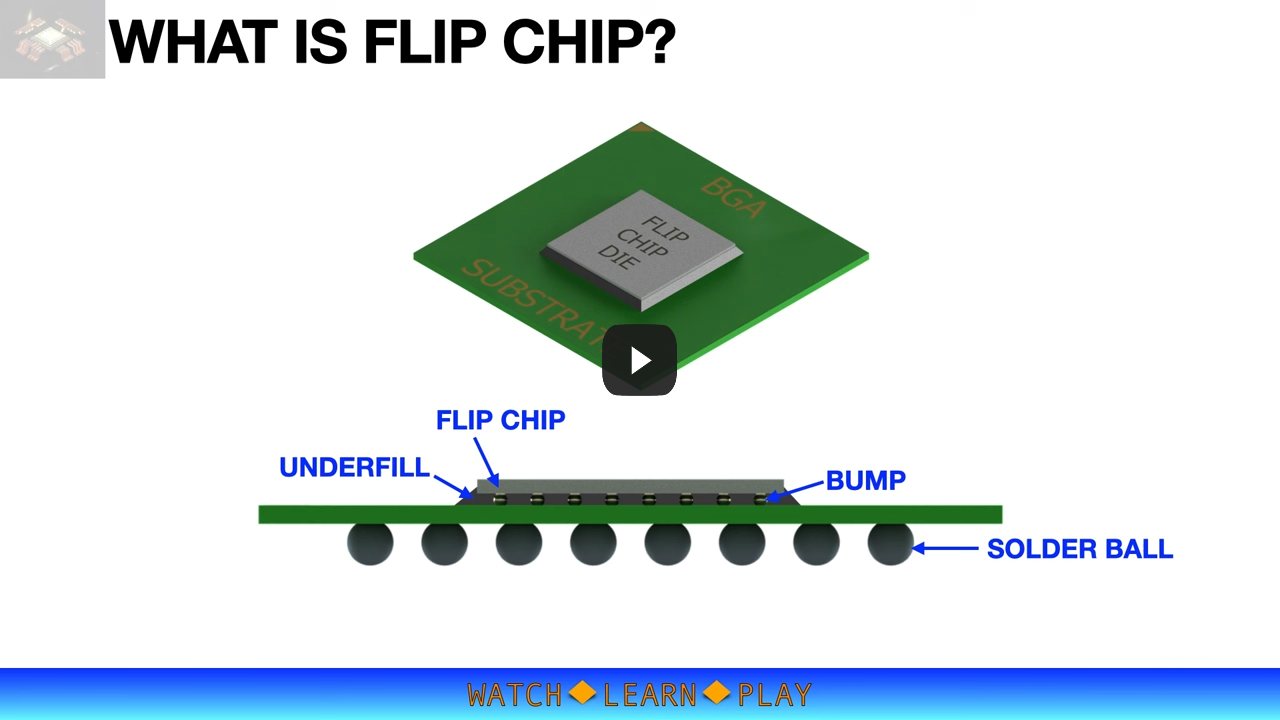 As one of the Top 20 EMS companies in the world, IMI has over 40 years of experience in providing electronics manufacturing and technology solutions.
We are ready to support your business on a global scale.
Our proven technical expertise, worldwide reach, and vast experience in high-growth and emerging markets make us the ideal global manufacturing solutions partner.
Let's work together to build our future today.
Other Blog